
What project owners need to know.
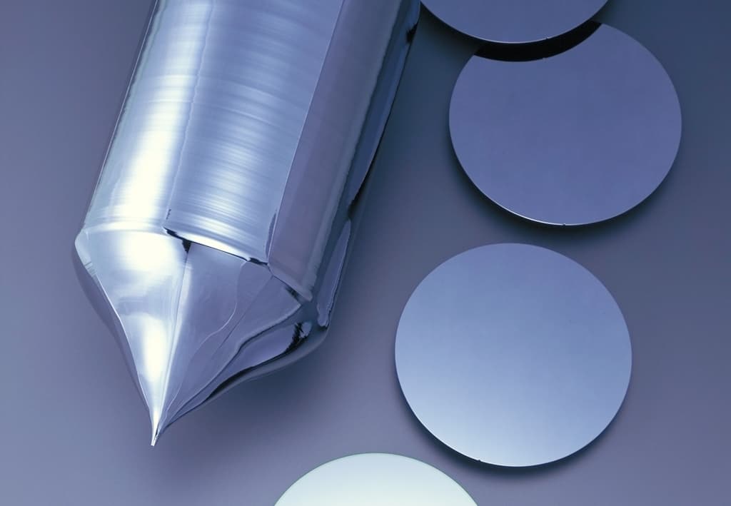
A kerfless wafer is a silicon wafer made without sawing it from an ingot, so none of the silicon is lost as sawdust (kerf). The two main routes are growing a thin crystalline layer from gas on a reusable seed and detaching it (epitaxial wafers), and forming a wafer directly from molten silicon. Both remain small or paused compared with the industry: as of late 2026, almost every solar cell is still built on a Czochralski-grown ingot sliced by diamond wire. Germany's NexWafe has reported epitaxial wafers performing close to CZ references in a heterojunction line, while US-based CubicPV paused its wafer factory plans in February 2024, citing a collapse in wafer prices.
Why anyone wants to skip the saw
Every sawn wafer pays a silicon tax. A 2024 review of diamond-wire saw silicon powder reports that roughly 35–45% of the silicon entering the slicing process leaves as fine waste particles in the cutting fluid. Diamond wire narrowed the cut compared with the older slurry process, but the loss is structural: a wire of finite thickness has to pass through the silicon.
The ingot route also carries energy and capital. Polysilicon is melted and regrown as a crystal over many hours in a Czochralski puller, then cropped, squared and sliced. A route that produced a wafer-thick crystal directly would, in principle, remove the puller, the saw and the kerf together. That is the promise kerfless technologies have chased for more than a decade.
- Kerf is a designed-in loss of the sawing route, not a tuning problem
- Kerfless routes aim to remove the puller, the saw and the kerf together
- The prize is lower silicon use per watt and fewer process steps
The two main kerfless routes
The first is the epitaxial or gas-to-wafer route. As TaiyangNews describes NexWafe's process, a reusable monocrystalline seed wafer is given a porous release layer, a new silicon layer is grown on it by atmospheric-pressure chemical vapour deposition, and the grown layer is detached as a free-standing wafer. The seed is then reused. Because the layer is grown to the target thickness, there is no slicing at all.
The second is direct-from-melt. 1366 Technologies, which later became part of CubicPV, developed a Direct Wafer process that formed wafers straight from molten silicon. CubicPV said the approach removed the ingot and sawing steps and could make a good bottom cell for tandem modules.
Older ribbon-growth methods, which pulled thin silicon sheets from a melt, belong to the same family. They reached commercial production in the past but were overtaken as sawn monocrystalline wafers fell in cost and rose in quality.
- Epitaxial: grow the wafer from gas on a reusable seed, then lift it off
- Direct-from-melt: form the wafer straight from molten silicon
- Ribbon growth: an earlier kerfless family, overtaken by sawn mono wafers
Where the companies actually got to
NexWafe is the most visible epitaxial player. pv magazine reported in 2023 that the Fraunhofer ISE spin-off was building toward commercial production in Germany, and TaiyangNews reported in 2025 that the company presented wafers reaching about 24.4% efficiency in a commercial heterojunction cell line, comparable to reference Czochralski wafers processed under the same conditions. Public reports differ on the size of its first factory, and we found no independent confirmation of volume output; any buyer should check current status directly with the company.
CubicPV went the other way. In February 2024, pv magazine USA and PV Tech reported that the company had halted plans for a 10 GW US wafer factory, citing a dramatic collapse in wafer prices and rising construction costs, and refocused on tandem module development. Notably, the US factory had been planned to start with conventional ingot-based mono wafers rather than Direct Wafer.
The pattern is consistent. Kerfless technologies have to beat a moving target: sawn CZ wafers that keep getting thinner, cheaper and better, made at enormous scale on mature, widely available equipment.
- NexWafe: epitaxial wafers reported near CZ performance in HJT; volume status unconfirmed
- CubicPV: US wafer factory paused in Feb 2024 on price collapse
- Sawn CZ wafers remain the moving benchmark kerfless must beat
Why sawn Czochralski wafers still dominate
Quality first. High-efficiency n-type cells such as TOPCon, heterojunction and back contact need long carrier lifetime and tight resistivity control. Czochralski growth, with magnetic-field and continuous-feed variants, delivers that at scale, and decades of process learning sit behind it.
Scale and supply chain second. Pullers, hot-zone graphite, quartz crucibles, diamond wire and slicers are produced in volume by many suppliers, and the know-how to run them is widespread. A kerfless line depends on far fewer equipment and material sources.
Price third. Wafer prices fell sharply in 2023 and 2024. A new technology has to win on cost against fully depreciated, very large incumbent plants, not against the wafer prices of the year it was designed.
- Lifetime and resistivity control at scale favour CZ
- Mature, multi-source equipment and consumables
- Incumbent cost base sets a very high bar for new routes
What it means for India's ingot and wafer plants
India is building ingot and wafer capacity now, with ALMM List-III bringing ingots and wafers into the approved-list regime from 1 June 2028. For plants being specified today, the practical choice is the Czochralski-plus-diamond-wire route, and the levers that matter are crucible quality, hot-zone control, wire and slicing discipline, and how much crop and kerf is recovered.
Kerfless technology is worth tracking rather than waiting for. If an epitaxial or direct-wafer route reaches proven volume with bankable cell results, it could change the economics of new capacity. Until then, the lower-risk path for an Indian plant is to make the sawn route as efficient as possible: thinner wafers, narrower wire, tight brick geometry, and segregated, traceable recycling of off-cuts.
- Specify CZ plus diamond wire for plants being built before 2028
- Track kerfless pilots; ask for independent cell data before acting
- Win today on crucible quality, hot-zone control and slicing discipline
How JRST supports this requirement
JRST Technology works across the silicon value chain, from high-purity quartz sand and quartz crucibles to ingot-wafer plant setup, equipment sourcing and spares. We help ingot and wafer projects specify the proven CZ-plus-diamond-wire route and keep watch on emerging technologies on their behalf. Buyers can browse wafer-line consumables and spares in the JRST Buyer Portal or on our silicon wafer products page. Figures here come from public sources and should be validated for each project.
Discuss your requirement
Mohammed Saif Zaveri connects JRST's industrial content to execution conversations.
As Co-Founder and designated partner of JRST Technology LLP, Mohammed Saif Zaveri works across industrial growth, strategic partnerships, client conversations, equipment strategy, and project pathways for silicon, solar, semiconductor, and advanced-manufacturing opportunities.
This knowledge page is part of JRST's public industrial knowledge base, designed to help buyers move from search terms and early research toward a structured technical-commercial discussion.
View Mohammed Saif Zaveri's profileConnect on LinkedInFrequently asked questions
What is a kerfless wafer?
A kerfless wafer is a silicon wafer made without sawing it from an ingot, so no silicon is lost as kerf powder. It is grown directly to wafer thickness, either from gas on a reusable seed (epitaxial) or directly from molten silicon.
Will kerfless wafers replace sawn ingots?
Not in the near term. As of late 2026, almost all solar cells use Czochralski ingots sliced by diamond wire. Kerfless routes have reported promising cell results but remain small, and at least one major effort, CubicPV's US wafer factory, was paused in 2024.
What is an epitaxial (EpiWafer) solar wafer?
It is a monocrystalline wafer grown by chemical vapour deposition on a reusable seed wafer that carries a porous release layer. The grown layer is detached as a free-standing wafer and the seed is reused, avoiding both the ingot and the saw.
Is kerf loss recoverable in sawn wafers?
Partly. Kerf leaves as sub-micron powder mixed with cutting fluid and metals, and published recovery routes reach around 5N purity, short of solar-grade. Solid off-cuts such as crop ends and squaring slabs are far easier to clean and remelt.
Should a new Indian wafer plant wait for kerfless technology?
No. Plants being built for ALMM List-III in June 2028 need proven equipment and bankable output. The practical route is Czochralski growth plus diamond-wire slicing, while tracking kerfless pilots for independent, volume-scale results.
Primary sources and further reading
Last reviewed 2026-11-20. Technical scope, policy eligibility, availability, and commercial terms should be independently confirmed for each project.