
What project owners need to know.
The carbon footprint of a solar module is the greenhouse gas emitted to make it, and for crystalline silicon most of it comes upstream: polysilicon refining is usually the largest single step, followed by wafer production, with cells and module assembly smaller. Because these steps run on electricity, the grid where each one happens can change the total as much as the technology does.
Why embodied carbon is now a procurement question
Carbon footprint used to be a sustainability report line. It is increasingly a buying condition. France has used a simplified carbon assessment, the Évaluation Carbone Simplifiée (ECS), in its solar tenders for years, and from 1 October 2025 its reduced 5.5 percent VAT rate for residential systems under 9 kW requires modules below 530 kgCO₂eq per kWp, InfoLink reported.
For Indian manufacturers looking at export markets, that means a module's carbon number can decide whether it is eligible at all. It also means the number has to be documented, stage by stage, back to the polysilicon.
A stage-by-stage view
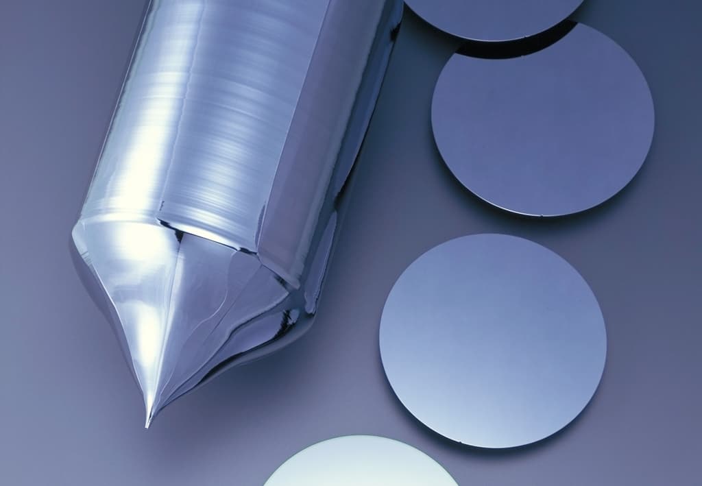
Quartz is first reduced to metallurgical-grade silicon in electric arc furnaces using carbon reductants, which releases CO₂ directly. That silicon is refined into polysilicon, typically by the energy-intensive Siemens process. Polysilicon is melted and grown into ingots, which are sliced into wafers; then come cells and modules.
An industry breakdown published by Sinovoltaics puts polysilicon refining at roughly 35–45 percent of manufacturing emissions, wafer production at about 15–20 percent, metallurgical silicon at 5–8 percent, and cells and module assembly at about 10–15 percent each. These are indicative estimates, not measured plant values, and they vary with technology and location. InfoLink, describing the French ECS method, reports that polysilicon production, the Siemens process and cell manufacturing together account for more than 60 percent of total emissions.
- MG-silicon: arc-furnace reduction of quartz (~5–8%, indicative)
- Polysilicon: usually the largest single step (~35–45%, indicative)
- Ingot and wafer: crystal growth and slicing (~15–20% for wafer, indicative)
- Cells and modules: ~10–15% each (indicative)
Why the grid and the process change the number
Most of these steps are electricity-intensive, so the carbon intensity of the local grid matters a great deal. A 2021 IEEE PVSC study by Annick Anctil found that making modules in China from US polysilicon reduced the footprint by about 9.5 percent compared with fully Chinese modules, and that manufacturing entirely in the US could reduce it by about 30 percent, reflecting regional electricity mix.
InfoLink's simulation for the French threshold makes the same point: a fully Chinese supply chain came out at about 574 kgCO₂eq/kWp, above the 530 limit, while switching to German polysilicon brought it to about 495. Process choices matter too. IEA PVPS's 2026 life cycle inventory update, built from 83 factory-level assessments gathered through the French tender process, reports more internally recycled silicon in ingot production, less kerf loss from thinner diamond wire, and a markedly lower environmental impact for the module supply chain than in its 2020 edition.
What a domestic supply chain can and cannot claim
A shorter supply chain cuts transport and gives better traceability, but it does not automatically mean lower carbon. If ingots are grown or polysilicon refined on a coal-heavy grid, the footprint can be higher than an imported equivalent made on cleaner power. For India, where grid mix differs by state and many plants are adding captive renewable power, the honest answer is that it depends on the site, the power contract and the process.
We do not publish carbon figures for JRST's own operations, and will do so only once they have been measured and verified under a recognised method. Any supplier making a low-carbon claim should be able to show the same.
What buyers should ask suppliers
A credible carbon claim is traceable and method-based. These questions separate a measured footprint from a marketing number.
- Which method was used (for example ISO 14067, or the French ECS), and who verified it?
- Where were the polysilicon, ingot and wafer made, and on what electricity supply?
- Is the figure for a specific product and factory, or an industry average?
- How are recycled silicon and kerf losses treated?
- When was the assessment done, and does it reflect the current supply chain?
How JRST supports this requirement
JRST works on the upstream steps where much of a module's footprint is set: high-purity quartz sand processing, crucible supply coordination and Maharashtra's first silicon-ingot line in Nagpur. We help project teams think about traceability, power and process efficiency alongside equipment. This guide summarises public estimates and reporting as of the date shown; it does not state JRST carbon figures. Stage shares are indicative and thresholds change, so confirm against the current official method and a verified assessment before making a procurement or investment decision.
Discuss your requirement
Mohammed Saif Zaveri connects JRST's industrial content to execution conversations.
As Co-Founder and designated partner of JRST Technology LLP, Mohammed Saif Zaveri works across industrial growth, strategic partnerships, client conversations, equipment strategy, and project pathways for silicon, solar, semiconductor, and advanced-manufacturing opportunities.
This knowledge page is part of JRST's public industrial knowledge base, designed to help buyers move from search terms and early research toward a structured technical-commercial discussion.
View Mohammed Saif Zaveri's profileConnect on LinkedInFrequently asked questions
What part of solar manufacturing emits the most carbon?
For crystalline silicon, polysilicon refining is usually the largest single step, with wafer production next. Industry estimates put polysilicon at roughly 35–45 percent of manufacturing emissions, though this varies by plant and grid.
Does local sourcing lower embodied carbon?
Not automatically. It depends on the carbon intensity of the electricity used at each stage and on process efficiency. Local sourcing improves traceability, but a low-carbon claim still has to be measured.
What is France's carbon threshold for solar modules?
For the reduced 5.5 percent VAT rate on residential systems under 9 kW, applied from 1 October 2025, modules must be below 530 kgCO₂eq per kWp, InfoLink reported. Tender rules have their own criteria; check the current CRE and ADEME documents.
How is a solar module's carbon footprint measured?
Through a life cycle assessment that counts emissions at each manufacturing stage, using a standard such as ISO 14067 or France's simplified carbon assessment, with factory-specific data where available.
Why does the electricity grid matter so much?
Polysilicon refining, crystal growth and wafering are electricity-intensive, so the same process run on a cleaner grid produces a lower footprint.
Primary sources and further reading
Last reviewed 2026-10-21. Technical scope, policy eligibility, availability, and commercial terms should be independently confirmed for each project.