
What project owners need to know.
A monocrystalline silicon ingot is one continuous crystal pulled from molten silicon by the Czochralski method, while a multicrystalline ingot is a block cast by directional solidification that contains many crystal grains with different orientations. Grain boundaries and dislocations in multicrystalline silicon lower cell efficiency, so the market has moved almost entirely to mono: Fraunhofer ISE's July 2026 Photovoltaics Report puts 2025 production at about 690 GWp mono-Si out of 706 GWp, and says multicrystalline technology has in practice disappeared from the market. Either kind of ingot is then sliced into wafers, the thin slices that become solar cells.
First, ingot vs wafer
A silicon ingot is the large crystalline block grown from molten polysilicon. A wafer is a thin slice cut from that ingot, which is then processed into a solar cell or a chip. One ingot yields many wafers, so ingot capacity sets the ceiling on how many wafers, and in turn cells and modules, a supply chain can make.
The choice between monocrystalline and multicrystalline is made at the ingot stage. It decides the crystal structure every downstream wafer inherits, and no later process step can turn a multicrystalline wafer into a single crystal.
How a monocrystalline ingot is grown
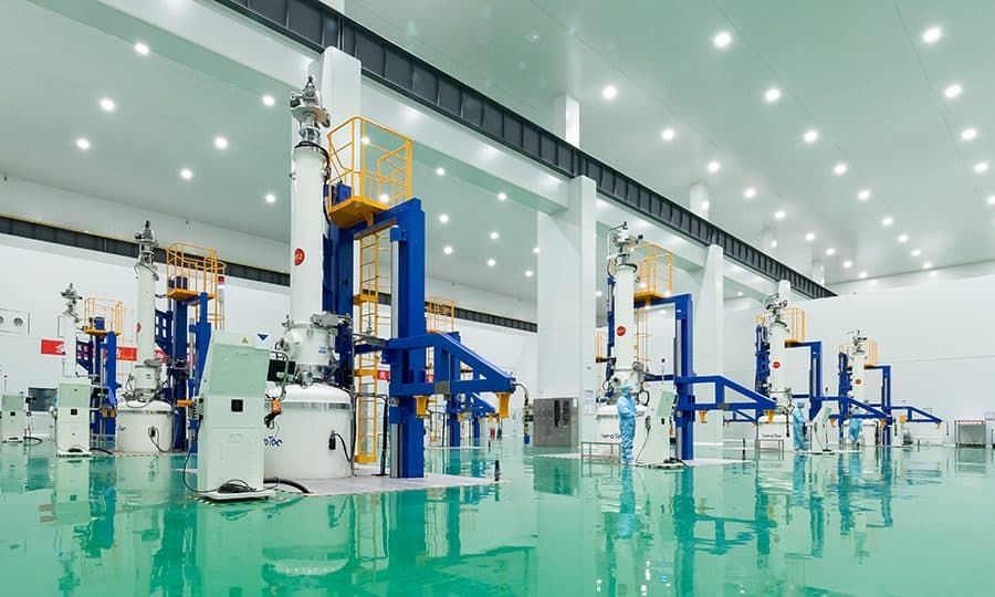
Monocrystalline solar ingots are grown by the Czochralski (Cz) method. PV-Manufacturing.org, the UNSW-led educational resource, describes the process: a single-crystal silicon seed is placed on the surface of the melt, rotated and slowly drawn upward, and the silicon that solidifies beneath it follows the seed's crystal structure, forming one continuous crystal. Temperature and pulling speed are tuned to eliminate dislocations, and the pulling speed also sets the crystal's diameter.
The result is a cylinder, which PV-Manufacturing.org gives as roughly 200 to 300 mm in diameter, later trimmed to a pseudo-square cross-section for solar wafers. The melt sits in a fused-quartz crucible, and the polysilicon charge is doped with phosphorus for n-type or gallium for p-type material.
- One continuous crystal following the seed's orientation
- Cylindrical ingot, trimmed to pseudo-square for solar wafers
- Melt held in a fused-quartz crucible; n-type doped with phosphorus
How a multicrystalline ingot is cast
Multicrystalline (mc-Si) ingots are made by directional solidification: the silicon is melted in a crucible and then cooled in a controlled way so that it freezes from the bottom upward. With no single seed setting the orientation, the block forms many grains, each with its own crystal orientation. PV-Manufacturing.org notes that this route is cheaper than Czochralski growth.
The crucible matters here too. A SunEdison patent on coated crucibles (US 9,458,551 B2, granted 2016) describes the conventional practice of coating silica crucibles with silicon nitride, partly so the solidified ingot can be released without cracking. PV-Manufacturing.org adds that during cooling, iron and other impurities migrate from the crucible into the ingot, creating a high-impurity 'red zone', and wafers from the outer region are often discarded.
Why the defects decide the outcome
The efficiency gap comes from the crystal structure. PV-Manufacturing.org lists the structural defects that form in multicrystalline growth: grain boundaries, dislocations, inclusions and oxides. Grain boundaries create recombination and shunt paths, and dislocations are particularly hard to neutralise in later processing, so they remain a major source of recombination. Metallic impurities such as iron add to the loss.
Producers narrowed the gap for a time with high-performance multicrystalline silicon, which uses seeding and careful cooling-rate control to grow small, uniform grains with fewer dislocation clusters. But a single crystal avoids grain boundaries altogether, and it suits the high-efficiency n-type cell designs the industry has moved to.
- Grain boundaries: recombination and shunt paths
- Dislocations: hard to passivate, a lasting efficiency loss
- Crucible-side impurities and edge losses reduce usable yield
The market verdict: mono, and now n-type mono
The shift is close to complete. Fraunhofer ISE's Photovoltaics Report (14 July 2026) lists 2025 production as about 690 GWp mono-Si, 16 GWp thin film and 0 GWp multi-Si, out of a 706 GWp total reported by ITRPV, and states that in practice multicrystalline silicon technology has disappeared from the market. As recently as ITRPV 2019, PV-Manufacturing.org notes, mc-Si held around 60% of cell production.
The same Fraunhofer report says silicon wafer-based technology made up about 98% of 2025 production, with an 86% share of n-type wafers according to ITRPV, and that monocrystalline n-type TOPCon has become dominant. In other words, the question for a new ingot plant today is not mono or multi, but how well it can grow n-type mono.
What this means for India
India is building ingot and wafer capacity ahead of ALMM List-III, which MNRE has announced for ingots and wafers from 1 June 2028. New capacity is being specified around Czochralski pullers, not casting furnaces, because that is what today's TOPCon and other n-type cell lines buy.
That shifts attention to the inputs that matter most for n-type Cz growth: crucible-grade quartz, polysilicon purity, oxygen control and resistivity uniformity along the ingot. These are process and qualification questions, and plants should plan validation runs before committing to volume output.
- Specify Cz pullers for n-type mono, matched to the target cell technology
- Treat crucible quality and polysilicon purity as ingot-quality inputs
- Plan oxygen and resistivity control into the puller and recipe specification
- Track ALMM List-III timing alongside ingot qualification
How JRST supports this requirement
JRST's team has hands-on experience of Czochralski ingot growth in silicon factories and helped deliver Maharashtra's first silicon-ingot pilot, and can support puller selection, crucible and consumable sourcing, and ingot-quality planning for Indian projects. Process outcomes are site- and recipe-specific and must be validated through qualification runs.
Discuss your requirement
Mohammed Saif Zaveri connects JRST's industrial content to execution conversations.
As Co-Founder and designated partner of JRST Technology LLP, Mohammed Saif Zaveri works across industrial growth, strategic partnerships, client conversations, equipment strategy, and project pathways for silicon, solar, semiconductor, and advanced-manufacturing opportunities.
This knowledge page is part of JRST's public industrial knowledge base, designed to help buyers move from search terms and early research toward a structured technical-commercial discussion.
View Mohammed Saif Zaveri's profileConnect on LinkedInFrequently asked questions
What is the difference between a silicon ingot and a wafer?
A silicon ingot is a large crystalline block grown from molten polysilicon, typically by the Czochralski method. A wafer is a thin slice cut from that ingot and processed into a solar cell or chip. One ingot yields many wafers, so ingot capacity sets the ceiling for wafer, cell and module output.
What is the difference between monocrystalline and multicrystalline silicon?
Monocrystalline silicon is a single continuous crystal, usually pulled by the Czochralski method. Multicrystalline silicon is cast by directional solidification and contains many grains with different crystal orientations, separated by grain boundaries.
Which gives higher efficiency, mono or multi?
Monocrystalline. Grain boundaries, dislocations and metallic impurities in multicrystalline silicon cause recombination losses, which is why mono wafers are used for high-efficiency cell designs such as TOPCon.
Why are monocrystalline ingots cylindrical?
A Czochralski crystal is pulled and rotated out of the melt, so it grows as a cylinder. For solar wafers the cylinder is trimmed to a pseudo-square cross-section before slicing.
Is multicrystalline silicon still used for solar?
Very little. Fraunhofer ISE's July 2026 Photovoltaics Report lists 0 GWp of multi-Si in 2025 production and says the technology has in practice disappeared from the market.
Do both methods use a crucible?
Yes. Czochralski growth holds the melt in a fused-quartz crucible, while directional solidification conventionally uses a silica crucible coated with silicon nitride to help release the solidified ingot. Crucible-side impurities affect ingot quality in both.
What is high-performance multicrystalline silicon?
A refined casting approach that uses seeding and controlled cooling to grow small, uniform grains with fewer dislocation clusters. It narrowed the gap with mono for a time before the market moved to n-type monocrystalline wafers.
Primary sources and further reading
Last reviewed 2026-10-13. Technical scope, policy eligibility, availability, and commercial terms should be independently confirmed for each project.